Microstructural analysis using scanning electron microscopy (SEM)
Unlocking the Secrets of Materials Microstructural Analysis using Scanning Electron Microscopy (SEM) with Eurolab
In todays fast-paced business world, staying ahead of the competition requires making informed decisions based on accurate and reliable data. This is particularly true for industries that rely heavily on materials science, such as aerospace, automotive, electronics, and pharmaceuticals. One crucial tool in the armory of any serious researcher or scientist is Microstructural analysis using Scanning Electron Microscopy (SEM). At Eurolab, our team of experts provides top-notch SEM services to help businesses unlock the secrets of their materials.
What is Microstructural Analysis using Scanning Electron Microscopy (SEM)?
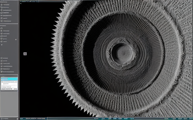
Scanning Electron Microscopy (SEM) is a non-destructive analytical technique that allows researchers to study the surface morphology and microstructure of materials at high resolutions. By combining high-resolution imaging with advanced spectroscopic capabilities, SEM provides unparalleled insights into the internal structure and composition of materials. This information is crucial for understanding material properties, optimizing processing conditions, and ensuring product quality.
Microstructural analysis using SEM involves carefully preparing a sample by coating it with a thin layer of electrically conductive material to prevent charging effects during imaging. The sample is then placed in the vacuum chamber of an SEM instrument, where it is bombarded with a focused beam of high-energy electrons. These electrons interact with the samples surface, producing signals that are used to create detailed images and gather information on elemental composition.
Why Microstructural Analysis using Scanning Electron Microscopy (SEM) is Essential for Businesses
The benefits of microstructural analysis using SEM extend far beyond the laboratory bench. By harnessing the power of SEM, businesses can
Improve Material Properties Identify defects, impurities, and structural irregularities that impact material performance.
Optimize Processing Conditions Refine manufacturing processes to achieve desired properties and reduce waste.
Enhance Product Quality Ensure compliance with industry standards and regulations through accurate analysis.
Reduce Costs Minimize the need for rework, scrap, or replacement due to material defects.
Accelerate Innovation Leverage SEMs advanced capabilities to explore new materials and applications.
Key Benefits of Microstructural Analysis using Scanning Electron Microscopy (SEM)
Our team at Eurolab has expertly honed the art of microstructural analysis using SEM. Here are some key benefits our clients have come to appreciate
High-Resolution Imaging Resolve details as small as 1-2 nanometers with precision and accuracy.
Advanced Spectroscopy Unravel elemental composition, chemical bonding, and molecular structures.
Non-Destructive Analysis Analyze samples without altering their physical or chemical properties.
Fast Turnaround Times Receive results quickly, often within hours or days, not weeks.
Expert Interpretation Our skilled analysts provide comprehensive reports and actionable insights.
How Microstructural Analysis using Scanning Electron Microscopy (SEM) Works
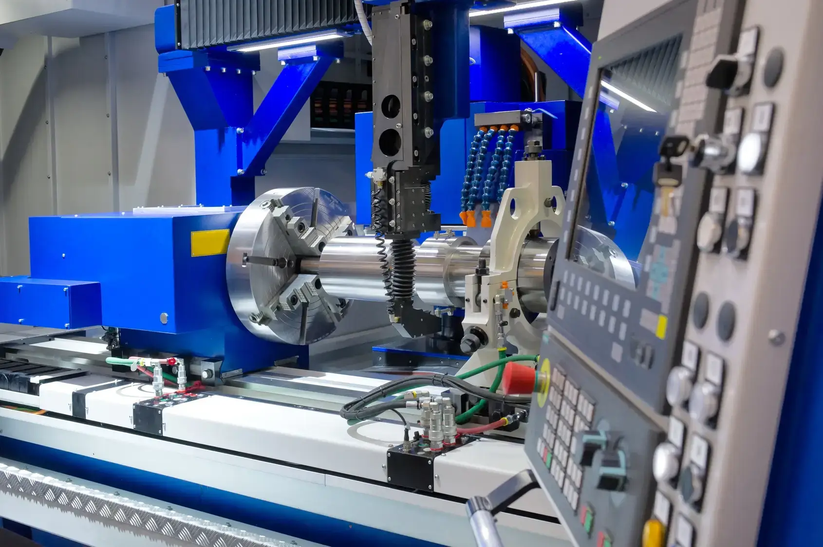
At Eurolab, our SEM services involve a carefully calibrated workflow
Sample Preparation Carefully prepare samples to ensure optimal imaging conditions.
Instrument Calibration Verify instrument performance and accuracy before analysis.
Data Acquisition Collect high-resolution images and spectroscopic data using advanced software tools.
Data Analysis Expertly interpret results, providing comprehensive reports and recommendations.
Frequently Asked Questions (FAQs)
Were often asked about the intricacies of microstructural analysis using SEM. Here are some common questions and answers
Q What types of materials can be analyzed using SEM?
A A wide range of materials can be analyzed, including metals, ceramics, polymers, composites, and biological samples.
Q How long does a typical analysis take?
A Turnaround times vary depending on the complexity of the project. Typically, results are available within hours or days.
Q Can SEM analyze internal structures of materials?
A Yes, with specialized techniques such as cross-sectional imaging and focused ion beam (FIB) milling.
Q What are the limitations of SEM analysis?
A While SEM provides unparalleled insights, it is not suitable for all types of samples. For example, biological samples may require additional preparation or alternative analytical methods.
Conclusion
Microstructural analysis using Scanning Electron Microscopy (SEM) is an indispensable tool in modern materials science research and development. At Eurolab, our team of experts has refined the art of SEM to provide unparalleled insights into material properties and behavior. By partnering with us, businesses can unlock the secrets of their materials, drive innovation, and stay ahead of the competition.
Dont let material mysteries hold you back any longer. Contact us today to learn more about how microstructural analysis using SEM can revolutionize your business!