SEM-EDS for elemental mapping of microstructures
Unlocking the Secrets of Microstructures How Eurolabs SEM-EDS Elemental Mapping Service Revolutionizes Material Analysis
In todays competitive business landscape, understanding the intricacies of materials and their microstructures is crucial for innovation, quality control, and product development. One powerful tool that enables businesses to gain a deeper insight into material composition is Scanning Electron Microscopy-Energy Dispersive Spectroscopy (SEM-EDS) elemental mapping. Eurolabs SEM-EDS service offers unparalleled precision in elemental analysis, empowering companies to make informed decisions, optimize processes, and drive growth.
What is SEM-EDS Elemental Mapping?
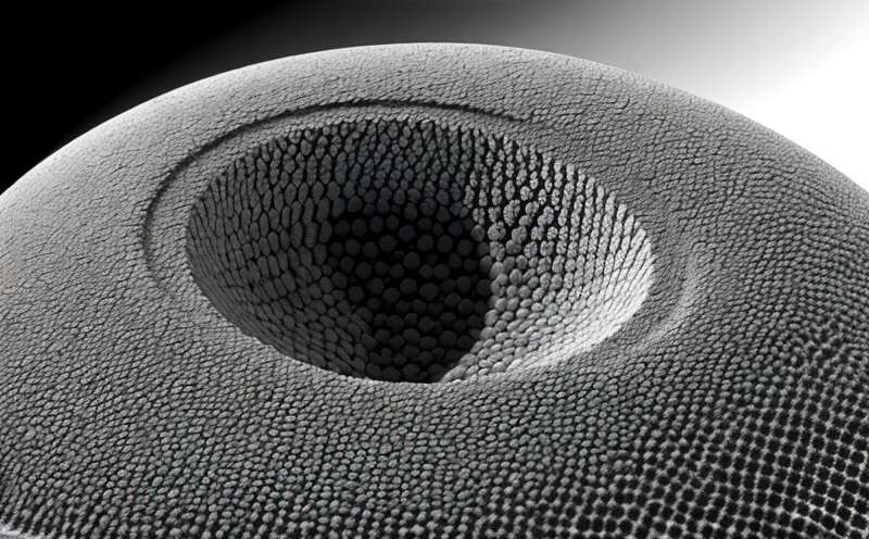
SEM-EDS is a non-destructive analytical technique that combines the high-resolution imaging capabilities of Scanning Electron Microscopy (SEM) with the chemical analysis prowess of Energy Dispersive Spectroscopy (EDS). This synergy allows for the simultaneous visualization and identification of elemental distributions within microstructures, providing an unparalleled understanding of material composition.
Why is SEM-EDS Essential for Businesses?
The benefits of using SEM-EDS for elemental mapping of microstructures are multifaceted
Advantages of SEM-EDS Elemental Mapping
Accurate and detailed elemental analysis SEM-EDS provides precise information on the presence, concentration, and distribution of elements within a material.
Non-destructive testing The technique allows for the examination of samples without causing damage or alteration to their structure.
High-resolution imaging SEM-EDS offers exceptional image resolution, enabling researchers to visualize microstructures with unprecedented clarity.
Multi-element analysis This technique can detect and analyze multiple elements simultaneously, streamlining the analytical process.
Quantitative results SEM-EDS provides accurate quantitative data on elemental concentrations, allowing for precise comparisons and measurements.
Cost-effective By identifying issues early in the production process, businesses can reduce costs associated with rework, scrap, or failure.
Improved product quality SEM-EDS helps manufacturers optimize material selection, processing conditions, and formulations to achieve consistent high-quality products.
Key Benefits for Various Industries
Materials Science Understanding microstructure and elemental composition is critical for developing new materials with improved properties. Eurolabs SEM-EDS service helps researchers identify optimal material combinations.
Manufacturing By analyzing product defects, manufacturers can implement corrective actions to prevent failures and improve efficiency.
Aerospace Accurate analysis of high-strength alloys and advanced composites ensures the reliability and safety of aircraft components.
Pharmaceuticals SEM-EDS helps identify contaminants and impurities in raw materials and finished products, ensuring compliance with regulatory standards.
QA Section
Q What is the minimum sample size required for SEM-EDS analysis?
A Eurolabs SEM-EDS system can analyze samples as small as 1 micrometer (μm) in diameter.
Q Can SEM-EDS be used to analyze wet or contaminated samples?
A While SEM-EDS is typically performed on dry, clean samples, our experienced technicians can prepare and analyze a wide range of materials, including those with complex surface characteristics.
Q How long does the analysis process take?
A The time required for SEM-EDS analysis depends on the complexity of the sample and the number of elements being analyzed. Our dedicated team will provide a detailed project timeline to ensure timely delivery of results.
Q Can I obtain raw data from the analysis?
A Yes, Eurolab provides clients with comprehensive reports, including elemental maps, spectra, and quantitative data. Raw data can also be made available upon request.
Conclusion
Eurolabs SEM-EDS service represents a significant advancement in material analysis, empowering businesses to optimize product development, quality control, and process efficiency. By harnessing the power of this cutting-edge technology, companies can unlock new opportunities for growth, innovation, and success.