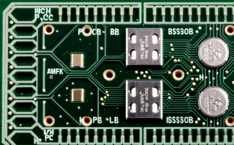
Assessing PCB Resistance to Wear and Tear
Assessing PCB Resistance to Wear and Tear The Key to Ensuring the Longevity of Your Products
In todays fast-paced business environment, companies are constantly looking for ways to improve efficiency, reduce costs, and minimize risks. One critical aspect that often gets overlooked is the reliability of their products components. Printed Circuit Boards (PCBs) are a crucial part of any electronic device, and their ability to withstand wear and tear can make all the difference between a products success or failure.
At Eurolab, our team of experts understands the importance of assessing PCB resistance to wear and tear. This laboratory service is designed to help businesses like yours identify potential weaknesses in their products components, allowing them to take proactive steps towards preventing costly failures and ensuring compliance with industry standards.
What is Assessing PCB Resistance to Wear and Tear?
Assessing PCB resistance to wear and tear involves subjecting printed circuit boards to various environmental stresses and conditions that mimic real-world use. This includes exposure to temperature fluctuations, humidity, vibrations, and other factors that can cause components to deteriorate over time. Our expert technicians then analyze the results to identify areas of weakness and provide recommendations for improvement.
Why is Assessing PCB Resistance to Wear and Tear Essential for Businesses?
There are several compelling reasons why assessing PCB resistance to wear and tear should be a top priority for businesses
Prevents Costly Failures By identifying potential weaknesses in your products components, you can take proactive steps to prevent costly failures that can result in lost sales, damaged reputation, and financial losses.
Ensures Compliance with Industry Standards Many industries have specific regulations and standards governing the reliability of electronic components. Assessing PCB resistance to wear and tear ensures compliance with these standards and minimizes the risk of non-compliance.
Reduces Warranty Claims By identifying potential weaknesses in your products components, you can reduce the likelihood of warranty claims and associated costs.
Improves Product Design The insights gained from assessing PCB resistance to wear and tear can be used to improve product design, making them more reliable, efficient, and cost-effective.
The Benefits of Assessing PCB Resistance to Wear and Tear
Here are some key benefits of using our laboratory service
Comprehensive Analysis Our expert technicians subject your printed circuit boards to a range of environmental stresses and conditions, providing a comprehensive analysis of their resistance to wear and tear.
Identifies Potential Weaknesses Our analysis identifies areas of weakness in your products components, allowing you to take proactive steps towards preventing costly failures.
Recommendations for Improvement Our team provides recommendations for improvement, ensuring that your products meet industry standards and are more reliable, efficient, and cost-effective.
Cost-Effective Solution Assessing PCB resistance to wear and tear is a cost-effective solution compared to the costs associated with product failures, warranty claims, and compliance issues.
How Does the Laboratory Service Work?
Our laboratory service involves the following steps
Sample Preparation Our team receives your printed circuit boards and prepares them for testing.
Environmental Stress Testing We subject your PCBs to a range of environmental stresses and conditions, including temperature fluctuations, humidity, vibrations, and more.
Analysis and Reporting Our expert technicians analyze the results and provide a comprehensive report highlighting areas of weakness and recommendations for improvement.
Frequently Asked Questions
Here are some common questions about our laboratory service
Q What types of printed circuit boards can be tested?
A We test a wide range of printed circuit boards, including those made from various materials, such as FR4, Rogers, and more.
Q How long does the testing process take?
A The testing process typically takes 1-3 weeks, depending on the complexity of the analysis.
Q What types of environmental stresses are tested?
A We subject your PCBs to a range of environmental stresses, including temperature fluctuations, humidity, vibrations, and more.
Q Can I get a sample report before committing to the full service?
A Yes, we can provide a sample report based on a small subset of samples. This allows you to see the quality of our analysis and recommendations.
Conclusion
Assessing PCB resistance to wear and tear is an essential step in ensuring the longevity and reliability of your products components. At Eurolab, our team of experts provides a comprehensive laboratory service that helps businesses like yours identify potential weaknesses and take proactive steps towards preventing costly failures and ensuring compliance with industry standards.
Dont risk the success of your business by overlooking this critical aspect of product development. Contact us today to learn more about our laboratory service and how it can benefit your company.